Stay connected If you would like details of our latest news, events and opportunities sent directly to your inbox, sign-up to receive the Sciontec e-newsletters.
What is a PCB?
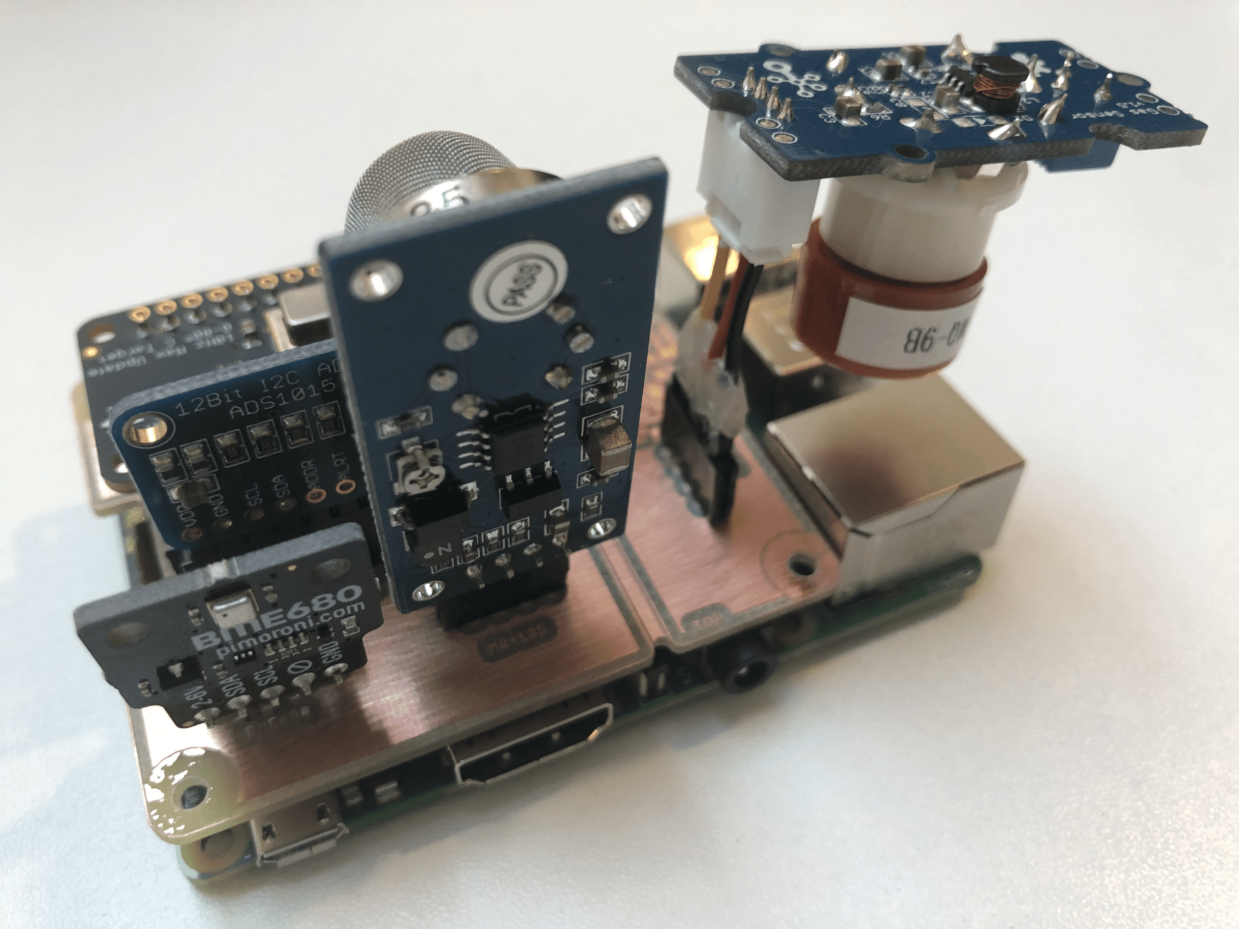
A printed circuit board (PCB) mechanically supports, and electrically connects, electrical components using conductive tracks, pads and other features, etched from one or more sheet layers of copper, laminated onto and/or between sheet layers of a non-conductive substrate.
Additionally, a PCB is no longer limited to a flat substrate, as Sensor City houses equipment capable of producing not only flexible circuit boards, but also conformal circuitry onto plastic parts, this allows complex electronics to be built into a variety of unusual locations, utilising wasted space inside product cases and housings.
PCB Design
Since CERN became key contributors to the code base of KiCAD, we’ve migrated the majority of our E-CAD operations to the KiCAD platform, and are able to conceptualise, design and iterate quickly using this powerful open-source software. Better yet, using an open-source platform allows us to share our work quickly and easily with our clients, further speeding up the design-evaluation cycle for electronics.
KiCAD is a powerful tool, with full 3D visualisation capability and a wide-range of common components ready to be used. It is also well supported with tutorial content via the common media sites.
Another great platform to watch is LibrePCB further demonstrating the open-source communities in-depth understanding and capability to develop powerful E-CAD software.
In-house Manufacture
At Sensor City, we can undertake PCB assembly in house within our state-of-the-art laboratories. Our PCB manufacturing and assembly equipment is from LPKF, a world leading brand in benchtop prototyping systems, and uses mixed milling and laser manufacture, to achieve track widths down to 50 micron, with a 15 micron separation.
Our LPKF systems work directly from CAD data which provides the necessary versatility for small prototype runs and test boards, our suite can also produce solder masks and stencils to simplify assembly of a working board. Through-hole plating and a multi-layer capability of up to 8 layers, completes our highly competent suite of equipment.
Our suite of LPKF equipment includes:
| LPKF EQUIPMENT | APPLICATION, FUNCTIONALITY & SPECIFICATION |
| Protolaser 3D | 3D circuit laser direct structure fabrication |
| Protomat D104 | Mechanical and Laser Machining |
| MultiPress S | Laminates rigid and flexible materials |
| Protoprint S | SMT stencil Printing and prints assembled double sided PCBs |
| ProLegend | Assembly layouts and solder resist masks |
| ProtoPlate LDS | Electrode-less 3D copper plating |
| ProtoPlace S & ProtoFlow S | Precise mounting of fine-pitch SMT components, process control and analysis |
LPKF Conformal Circuits
Our LPKF Protolaser 3D is one of only two machines publicly facing in the UK. As such, our engineers are highly trained to use this very specialised equipment to produce conformal electronics onto injection moulded or 3D printed parts.
Why undertake PCB Design in Liverpool?
The benefits of undertaking PCB manufacturing from our purpose-built innovation hub in Liverpool include reduced R&D time, and subsequently time to market, and the flexibility to adjust and fine tune design and production within one location.
Having all the PCB board production facilities in one UK lab facility like Sensor City also allows the production of more security conscious products, as we can facilitate a truly information-controlled service, ensuring complete confidentiality and control of informational flow throughout the PCB manufacturing process.


